Intel announces 32-layer 3D NAND chips, plans for larger-than-10TB SSDs
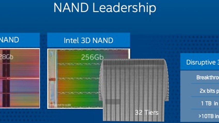
According to Intel, its 256-gigabit MLC NAND chips will consist of 32 layers, and will also be available in a 384-gigabit TLC configuration. Intel is claiming that its own 256Gb die sets efficiency records, but as Anandtech reports, this depends on how you count — Samsung has consciously chosen to use a 32-layer 86Gbit die to minimize its die foot print, as opposed to maximizing capacity. This gives Samsung’s V-NAND the smallest die size of any product currently on the market, with size being a very important factor in many markets.
Moving back up the nanometer ladder
Intel, like Samsung, is expected to announce that it uses a much larger process node for its 3D NAND. In Samsung’s case, it uses a 40nm process for 3D NAND, despite the fact that its working on 14nm planar technology for both logic and DRAM devices. Intel and Micron have already launched 16nm 2D NAND, but the fundamental characteristics of flash mean that device reliability decreases as process nodes shrink.
Intel's 3D NAND
Moving back up to 40nm NAND gave Samsung enough headroom to launch the fastest, most reliable SSD on the market today — the 850 Pro — and it’s expected to give Intel a similar kick. Intel isn’t willing to put a strict timetable on its plans for a 10TB SSD (and you can expect any such device to debut with an enterprise-class price tag), but Samsung has talked about stacking over a hundred layers of NAND per die — and if Intel hits equivalent densities, a 10TB SSD should be possible within five years.
Endurance-vs-Longevity
As the chart shows, moving back up to the 32nm node would more than double reliability as compared to 16nm levels. It also allows for less error correction, at least in theory, and might even enable increased drive densities. TLC drives have struggled to improve their Program/Erase (P/E) cycles, but a 40nm TLC drive might be able to offer the same reliability as an MLC drive at 16nm. The bottom line is, moving back to old nodes offers better options if density can still be scaled.
Ideally, researchers would find ways to adopt older process node technology for more than just NAND flash. The difficulty of building ever-smaller structures has gotten to the point that we’re bumping up against the physical limits of reality — next-generation EUV lithography has bogged down in no small part because the degree of perfection required at every stage of the manufacturing process is orders of magnitude above what the chip industry was previously required to achieve.
Intel is likely to roll out 3D NAND for enterprise SSDs first, but we should see consumer drives launching thereafter. With both Samsung and Intel on-board with the new technology, manufacturers like Toshiba are likely to follow in fairly short order.

